In 1953, the Darlington transistor or Darlington pair was introduced by the United States Electrical Engineer namely “Sidney Darlington”. It is configured by connecting two transistors together, which means, the emitter terminal of one transistor is applied as bias current to another transistor. There are different types of Darlington transistors based on polarity, the amount of power dissipation, collector current, package, CE voltage, and many more. This article gives a brief description of the 2N5306 NPN Darlington transistor, specifications, circuit diagram, working with applications.
What is 2N5306 NPN Darlington Transistor?
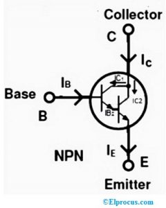
The 2N5306 NPN Darlington Transistor is designed by connecting two transistors together. One is NPN and the other is a PNP transistor combined in one package and looks like a normal transistor with the emitter, base, and collector terminals. It provides a high current gain when compared to a normal transistor.
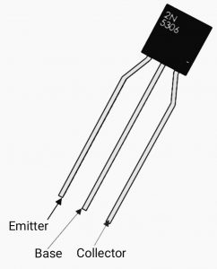
It is used in various applications of power regulators, audio amplifiers, motor control units, and many more. The 2N5306 NPN Darlington transistor available in the TO-92 package with three terminals such as emitter, base, and collector is shown in the figure below.

The main specification of the NPN Darlington transistor is its high current gain and high collector current (continuous). It shows the amplification of load current based on the input current of the base terminal. When the input current is applied to the base terminal of the transistor, then it is turned ON to allow the flow of the load current. The formula of load current when the transistor is in ON condition is,
Load Current = Input Current x Transistor Gain
When the load requires high power, it is necessary to increase the base current of the transistor. In some applications, the base current is limited and can’t be increased to increase the gain of the transistor. In this case, the Darlington transistor is used.
The 2N5306 is normally called an NPN Darlington transistor with a current gain of around 20000, which makes it very easy to use in amplifier applications. The maximum current allowed to pass through it is up to 1.2Amps, which helps to use in ideal applications of high current. The main drawback of the NPN Darlington transistor is the high base voltage of around 1.5 Volts.
Pin Configuration/Pin Diagram
The 2N6306 NPN Darlington Transistor pin configuration/pin diagram is illustrated below.

- Pin 1: (Emitter): This pin refers to an emitter pin, which is generally connected to the ground to drain out the current flowing through the transistor.
- Pin 2: (Base): This pin refers to the base pin, which is used to switch the transistor ON or OFF. It can control the transistor biasing.
- Pin 3: (Collector): This pin refers to a collector pin or terminal, which is connected to load. The current flows through this pin.
Features & Specifications
The following are the technical features or technical specifications of a 2N5306 NPN Darlington transistor.
- It is an NPN type of Darlington transistor available on the To-92 package with 3-pins-Emitter, Base, and Collector.
- The typical value of DC current gain (hfe) is high – 20,000 (minimum) and 70,000 (maximum) @ collector current Ic = 100 mAmps.
- The maximum Emitter to Base voltage (VBE) is 1.5 Volts
- The maximum continuous collector current (Ic) is 1.2 Amps
- The maximum collector to emitter voltage (VCE) is 25 Volts
- The maximum collector to base voltage (VCB) is 25 Volts
- The maximum power dissipation is 625mW (at above 25°C- 5mW/°C)
- The maximum junction to case thermal resistance is 83.3°C/W.
- The maximum junction to ambient thermal resistance is 200°C/W.
- The minimum collector to emitter breakdown voltage at Ic= 10 mA, IB= 0 is 25 Volts.
- The minimum collector to the base-emitter voltage at Ic =0.1microAmps, IE= 0 is 25V
- The minimum emitter to base breakdown voltage at IE= 0.1microAmps, IC=0 is 12V
- The maximum cut-off collector current at VCB = 25V, I=0 is 0.1 microamps and 20microamps @T=100°C
- The maximum cutoff emitter current at VEB=12V, IC=0 is 0.1microamps
- The minimum collector to emitter saturation voltage is 1.4V @ IC= 200mA, IB = 0.2mA
- The minimum base to emitter saturation voltage is 1.6V @ IC = 200mA, IB = 0.2mA
- The maximum collector to base capacitance is 10pF @ VCB=10V, f=1.0MHz
- The small-signal current gain is a maximum of 7,000 @ IC= 2mA, VCE = 5V, f= 1kHz and 6.0 @ IC= 2mA, VCE = 5V, f=10MHz.
- The minimum range of storage junction and operating temperature is -55°C to +150°C.
Alternatives of 2N5306 NPN Darlington Transistor are; BC636, BC639, BC549, BC547, 2N3055, 2N2369, 2N3906, 2N3904, 2N551, and 2SC5200 and an equivalent of a 2N5306 NPN Darlington Transistor is 2N5308.
How to Choose a Darlington Transistor?
A Darlington Transistor is selected in an application where a high current gain and amplification are required. This is because a normal BJT provides limited current gain. Sziklai Darlington pair or cross Darlington configuration is mainly used in Class AB amplifiers and push-pull topologies.
When to use a Darlington Transistor?
The Darlington Transistor is used in several applications where the high current gain with limited frequency response is required. When the base current is limited and can’t be increased to increase the gain of the transistor, then the Darlington transistor is used.
What are the Distinct Characteristics of 2N5306 NPN Darlington Transistors?
The distinct technical characteristics of a 2N5306 NPN Darlington Transistor are,
- Collector-base voltage VCBO: 25V
- Collector-emitter voltage VCEO: 25V
- Emitter-base voltage VEBO: 12V
- Thermal resistance: 200°C/W
- Power dissipation : 625mW
How to use 2N5306 NPN Darlington Transistor/Circuit Diagram?
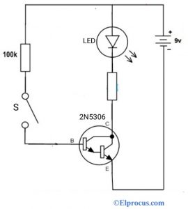
The Darlington transistors are widely used in amplification and switching applications to supply high DC current gain. Now let’s know how to use the 2N5306 NPN Darlington transistor as a switch from the following circuit diagram. The required electronic components to design the circuit are given below.

- LED
- 2N5306 NPN Darlington transistor
- Switch
- 100K resistor
- Supply 9V
Connect the circuit as shown in the diagram above. The LED is connected with the Darlington transistor. The switch is connected at the base terminal of the transistor along with that sensor to operate the LED. To protect the Darlington transistor, the 100K resistor is connected.
If the switch is closed, then the voltage greater than 1.4 volts is applied to the Darlington transistor, which becomes active and allows the current to pass through the load. Due to this, the LED is turned ON and light is emitted with high intensity irrespective of resistance at the base terminal.
If the switch is turned OFF, then the transistor operates in cut-off mode and the current passing through the load is zero. This makes the LED to be in OFF condition.
Where to Use/Applications
The application of 2N2306 NPN Darlington Transistor is given below,
- It is used in the switching of loads with high current (around 51)
- Used in signal gain boosters
- Used in audio amplifiers.
- Used as medium power switches
- Used in various circuits to achieve high amplification
- Used in rectifiers and other inverter circuits.
Please refer to this link to know more about 2N5306 NPN Darlington Transistor Datasheet
Thus, the NPN 2N6306 Darlington transistors provide high current gain and switches easily from high input impedance to low input impedance and vice versa. It is designed with two transistors in a single casing and requires fewer components to configure. Here is a question for you, “What are the advantages of 2N5306 NPN Darlington Transistors? “


0 Comments